David Savastano, Editor03.24.22
Conductive inks are a key market for flexible and printed electronics, as they essentially are responsible for the conductivity. It is a sizable market, with photovoltaics the largest end use. It is also a growing segment.
Dr. Matthew Dyson, senior analyst for IDTechEx, places the conductive ink segment at more than $2 billion.
“IDTechEx estimates the current conductive ink market size as $2.3 billion,” said Dr. Dyson. “Almost 80% is silver flake-based ink that is used to make the conductive fingers on silicon solar panels. While the market for this application established and may even decline in future as new technologies are adopted, there is extensive growth in flake-based inks for other applications, and also in emerging categories of conductive inks such as nanoparticle-based and particle-free inks.”
Khasha Ghaffarzadeh of TechBlick noted that the conductive ink market is extremely diverse and is thus hard to characterize as a single uniform entity. He added that the bulk of sales and revenue are still in established applications such as photovoltaics, membrane switches, touch electrodes, heaters and others.
“However, there are many exciting new applications, which bring with them new requirements as well as new opportunities, and will be the growth areas of the future,” added Ghaffarzadeh.
“In general, it is sometimes more useful to think of emerging sought-after features showing a high degree of commonality across many new applications,” Ghaffarzadeh observed. “I think formability of inks in general is an important feature these days, as it enables 3D and in-mold electronics as well as stretchable electronics for e-textiles, conformal sensors, wearable sensors, etc.
Nikhil Pampatwar, head of research and market intelligence for Verified Market Research, said that Verified Market Research estimates that the global conductive ink market for 2020 stood at USD$2.91 billion and is expected to grow at a CAGR of around 4% until year 2028, reaching a market value of USD$3.98 billion.
“Conductive ink supply is used for printed photovoltaic solar cells, exterior automotive heating applications and edge electrodes for touch screens,” Pampatwar added. “Growth from the automotive industry is likely to drive the overall conductive ink market as it’s a big growth market for conductive ink suppliers. In automotive industry flexible electronics can be used in displays, special sensors, contactless sensing for vehicles. The application is also relevant for electric vehicles.”
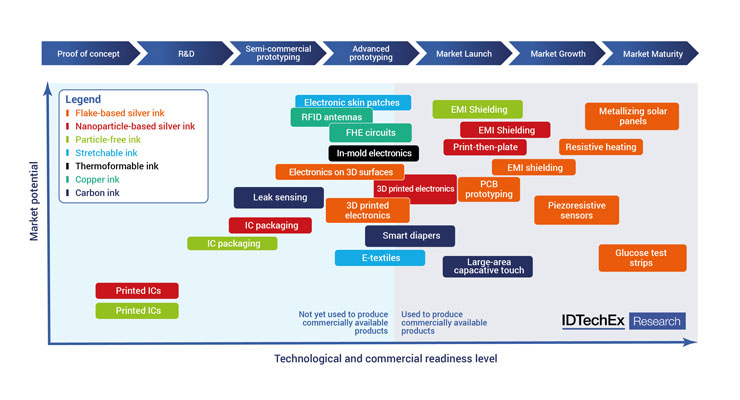
“In the near term the biggest growth opportunities would appear to be wearable electronic skin patches and in-mold electronics,” Dr. Dyson reported. “Electronic skin patches require stretchable conductive ink, along with printed conductive electrodes in many cases and are projected by IDTechEx to reach a market size of $38 billion by 2030.
Dr. Dyson said that in-mold electronics (IME), and the closely related film-insert molding, is another application opportunity.
“Integrating electronics within plastic panels reduces weight, complexity, and assembly costs,” he added. “IME is thus highly applicable to automotive interiors, household appliances and even some consumer goods.”
“Towards the end of the decade, we see applications in partially additive electronics manufacturing, for example printing wiring onto existing 3D structures, and of course in smart packaging,” Dr. Dyson added. “Even further into the future, electromagnetic meta-surfaces that assist in the propagation and directing of the higher frequencies that will be used for telecommunications may represent a huge market for conductive ink.”
Biggest Needs
Dr. Dyson said that the wide variety of applications for printed electronics means that there are many opportunities for differentiation within conductive inks, but there is much to be done.
“Wearable electronics require inks that are stretchable to various extents and can withstand repeated mechanical flexing. The requirements for IME are slightly different, in that inks need to withstand the temperature and pressure associated with thermoforming,” said Dr. Dyson.
“Considering conductive inks more broadly, the main challenges are durability and cost,” added Dr. Dyson. “Utilizing printed inks in harsh environments, such as automotive applications, means that they need to withstand repeated thermal cycling from -40 °C to 80°C, while of course silver-based inks are vulnerable to metal price rises.”
Ghaffarzadeh noted that the trend towards higher conductivity is a mainstay of the industry.
“People always want to get as close to bulk material as possible, and thus make a more efficient use of a given mass of silver or copper material,” Ghaffarzadeh noted. “In general, if one can sinter the material so that it becomes void- and residue-free with excellent particle packing, then one approaches bulk metal conductivity. This is generally hampered by the need to add binders, adhesion promoters, viscosity adjusters, softness adjusters, as well as by irregular particle shapes and limited curing temperature and time to eliminate all residues.
“In some cases, to prevent particle agglomeration or comply with the low viscosity requirements of the printing technique, the filler loading is kept low,” he added. “Improving on any of these features will improve the conductivity. To see how good one can get, it might be useful to look at sintered type silver or copper pastes used as die attach in power electronics. These sintered pastes behave very much like bulk material in terms of electrical and thermal conductivity.”
Ideal Materials for Conductive Inks and Paste
Silver remains by far the dominant material due to its high conductivity and resistance to oxidation. Dr. Dyson said the ideal material would be highly conductive, inexpensive, and chemically stable, but achieving all three simultaneously is very challenging.
“Both carbon nanotubes and graphene-based inks have been discussed as alternatives to silver, but thus far have experienced little traction as direct replacements,” Dr. Dyson pointed out. “Instead, they are more likely to find success in niche applications when silver ink is unsuitable. This could be due to a requirement for transparency, specific mechanical properties, or if there are concerns about the sustainability of silver once the product is disposed of.”
Dr. Dyson said that significant progress is being made on conductive copper inks, which offer both cost and sustainability benefits relative to silver.
“Utilizing copper hydride to generate an inert atmosphere in-situ enables oxidation to be avoided during deposition/sintering, but printed copper traces will require excellent encapsulation to prevent oxidation once incorporated into a product,” added Dr. Dyson.
Ghaffarzadeh said that copper has a long story of development in printed electronics.
“The newer generation of copper inks show great promise,” Ghaffarzadeh said. “The conductivity is better, and crucially there is good data on reliability, ease of sintering/curing as well as a good degree of solder compatibility. These are important milestones that enable the material to be adopted. In other words, if the performance is good and the ink is almost a drop-in replacement, and the cost is lower, then replacement can start.”
Pampatwar said that metal-based conductive inks are preferred as they have higher electrical/thermal conductivities compared to polymers and carbon-based inks.
“Silver is more commonly used in printing of electronic products, due to its excellent properties such as high electrical and thermal conductivity, and chemical stability,” Pampatwar said. “Similar to silver, other metals such as gold and copper are among the metals used as conductive inks. But high intrinsic thermal conductivity and cost effectiveness of copper makes it a better choice in making conductive inks compared to silver.
“However, with changing time and increasing cost of the silver, several new materials such as graphene, carbon nanotubes, copper or copper oxide, conductive zinc, and others are gaining attention,” Pampatwar added. “Polymer and carbon-based conductive inks have flexibility and extensibility and thus are more preferred in the flexible electronics. Carbon-based nanomaterial inks show huge potential in printed electronics application as they are electrically heterogeneous.”
The Future for Conductive Inks
Generally speaking, it seems like there are more products featuring printed and flexible electronics that are reaching the marketplace, and conductive inks are finding traction as well.
“There is substantial overlap between the most promising markets for printed/flexible electronics and for conductive inks,” Dr. Dyson said. “As such, electronic skin patches and in-mold electronics are especially promising applications in the near and medium term, while smart packaging is a compelling long-term prospect.
“Flexible hybrid electronics (FHE) is another exciting opportunity for conductive ink, since it will enable printed inks to be utilized within circuits that combine mounted components with printed conductive traces, and thus can replace PCBs for applications where flexibility and light weight are important,” added Dr. Dyson. “IoT devices are also a highly promising market, since they are likely to require both printed/flexible sensors and energy harvesting technologies such as indoor organic photovoltaics.”
“There are many industries where conductive inks found wide variety of advantages such as e-textiles, for instance, where conductive inks can be applied after the main product has been produced,” Pampatwar said. “The automotive industry is the next big market for conductive ink suppliers. A key trend here is transparent and efficient larger-area heating to eliminate the visible defroster lines.”
Dr. Matthew Dyson, senior analyst for IDTechEx, places the conductive ink segment at more than $2 billion.
“IDTechEx estimates the current conductive ink market size as $2.3 billion,” said Dr. Dyson. “Almost 80% is silver flake-based ink that is used to make the conductive fingers on silicon solar panels. While the market for this application established and may even decline in future as new technologies are adopted, there is extensive growth in flake-based inks for other applications, and also in emerging categories of conductive inks such as nanoparticle-based and particle-free inks.”
Khasha Ghaffarzadeh of TechBlick noted that the conductive ink market is extremely diverse and is thus hard to characterize as a single uniform entity. He added that the bulk of sales and revenue are still in established applications such as photovoltaics, membrane switches, touch electrodes, heaters and others.
“However, there are many exciting new applications, which bring with them new requirements as well as new opportunities, and will be the growth areas of the future,” added Ghaffarzadeh.
“In general, it is sometimes more useful to think of emerging sought-after features showing a high degree of commonality across many new applications,” Ghaffarzadeh observed. “I think formability of inks in general is an important feature these days, as it enables 3D and in-mold electronics as well as stretchable electronics for e-textiles, conformal sensors, wearable sensors, etc.
Nikhil Pampatwar, head of research and market intelligence for Verified Market Research, said that Verified Market Research estimates that the global conductive ink market for 2020 stood at USD$2.91 billion and is expected to grow at a CAGR of around 4% until year 2028, reaching a market value of USD$3.98 billion.
“Conductive ink supply is used for printed photovoltaic solar cells, exterior automotive heating applications and edge electrodes for touch screens,” Pampatwar added. “Growth from the automotive industry is likely to drive the overall conductive ink market as it’s a big growth market for conductive ink suppliers. In automotive industry flexible electronics can be used in displays, special sensors, contactless sensing for vehicles. The application is also relevant for electric vehicles.”
“In the near term the biggest growth opportunities would appear to be wearable electronic skin patches and in-mold electronics,” Dr. Dyson reported. “Electronic skin patches require stretchable conductive ink, along with printed conductive electrodes in many cases and are projected by IDTechEx to reach a market size of $38 billion by 2030.
Dr. Dyson said that in-mold electronics (IME), and the closely related film-insert molding, is another application opportunity.
“Integrating electronics within plastic panels reduces weight, complexity, and assembly costs,” he added. “IME is thus highly applicable to automotive interiors, household appliances and even some consumer goods.”
“Towards the end of the decade, we see applications in partially additive electronics manufacturing, for example printing wiring onto existing 3D structures, and of course in smart packaging,” Dr. Dyson added. “Even further into the future, electromagnetic meta-surfaces that assist in the propagation and directing of the higher frequencies that will be used for telecommunications may represent a huge market for conductive ink.”
Biggest Needs
Dr. Dyson said that the wide variety of applications for printed electronics means that there are many opportunities for differentiation within conductive inks, but there is much to be done.
“Wearable electronics require inks that are stretchable to various extents and can withstand repeated mechanical flexing. The requirements for IME are slightly different, in that inks need to withstand the temperature and pressure associated with thermoforming,” said Dr. Dyson.
“Considering conductive inks more broadly, the main challenges are durability and cost,” added Dr. Dyson. “Utilizing printed inks in harsh environments, such as automotive applications, means that they need to withstand repeated thermal cycling from -40 °C to 80°C, while of course silver-based inks are vulnerable to metal price rises.”
Ghaffarzadeh noted that the trend towards higher conductivity is a mainstay of the industry.
“People always want to get as close to bulk material as possible, and thus make a more efficient use of a given mass of silver or copper material,” Ghaffarzadeh noted. “In general, if one can sinter the material so that it becomes void- and residue-free with excellent particle packing, then one approaches bulk metal conductivity. This is generally hampered by the need to add binders, adhesion promoters, viscosity adjusters, softness adjusters, as well as by irregular particle shapes and limited curing temperature and time to eliminate all residues.
“In some cases, to prevent particle agglomeration or comply with the low viscosity requirements of the printing technique, the filler loading is kept low,” he added. “Improving on any of these features will improve the conductivity. To see how good one can get, it might be useful to look at sintered type silver or copper pastes used as die attach in power electronics. These sintered pastes behave very much like bulk material in terms of electrical and thermal conductivity.”
Ideal Materials for Conductive Inks and Paste
Silver remains by far the dominant material due to its high conductivity and resistance to oxidation. Dr. Dyson said the ideal material would be highly conductive, inexpensive, and chemically stable, but achieving all three simultaneously is very challenging.
“Both carbon nanotubes and graphene-based inks have been discussed as alternatives to silver, but thus far have experienced little traction as direct replacements,” Dr. Dyson pointed out. “Instead, they are more likely to find success in niche applications when silver ink is unsuitable. This could be due to a requirement for transparency, specific mechanical properties, or if there are concerns about the sustainability of silver once the product is disposed of.”
Dr. Dyson said that significant progress is being made on conductive copper inks, which offer both cost and sustainability benefits relative to silver.
“Utilizing copper hydride to generate an inert atmosphere in-situ enables oxidation to be avoided during deposition/sintering, but printed copper traces will require excellent encapsulation to prevent oxidation once incorporated into a product,” added Dr. Dyson.
Ghaffarzadeh said that copper has a long story of development in printed electronics.
“The newer generation of copper inks show great promise,” Ghaffarzadeh said. “The conductivity is better, and crucially there is good data on reliability, ease of sintering/curing as well as a good degree of solder compatibility. These are important milestones that enable the material to be adopted. In other words, if the performance is good and the ink is almost a drop-in replacement, and the cost is lower, then replacement can start.”
Pampatwar said that metal-based conductive inks are preferred as they have higher electrical/thermal conductivities compared to polymers and carbon-based inks.
“Silver is more commonly used in printing of electronic products, due to its excellent properties such as high electrical and thermal conductivity, and chemical stability,” Pampatwar said. “Similar to silver, other metals such as gold and copper are among the metals used as conductive inks. But high intrinsic thermal conductivity and cost effectiveness of copper makes it a better choice in making conductive inks compared to silver.
“However, with changing time and increasing cost of the silver, several new materials such as graphene, carbon nanotubes, copper or copper oxide, conductive zinc, and others are gaining attention,” Pampatwar added. “Polymer and carbon-based conductive inks have flexibility and extensibility and thus are more preferred in the flexible electronics. Carbon-based nanomaterial inks show huge potential in printed electronics application as they are electrically heterogeneous.”
The Future for Conductive Inks
Generally speaking, it seems like there are more products featuring printed and flexible electronics that are reaching the marketplace, and conductive inks are finding traction as well.
“There is substantial overlap between the most promising markets for printed/flexible electronics and for conductive inks,” Dr. Dyson said. “As such, electronic skin patches and in-mold electronics are especially promising applications in the near and medium term, while smart packaging is a compelling long-term prospect.
“Flexible hybrid electronics (FHE) is another exciting opportunity for conductive ink, since it will enable printed inks to be utilized within circuits that combine mounted components with printed conductive traces, and thus can replace PCBs for applications where flexibility and light weight are important,” added Dr. Dyson. “IoT devices are also a highly promising market, since they are likely to require both printed/flexible sensors and energy harvesting technologies such as indoor organic photovoltaics.”
“There are many industries where conductive inks found wide variety of advantages such as e-textiles, for instance, where conductive inks can be applied after the main product has been produced,” Pampatwar said. “The automotive industry is the next big market for conductive ink suppliers. A key trend here is transparent and efficient larger-area heating to eliminate the visible defroster lines.”
