David Savastano, Editor04.15.21
Conductive inks and pastes are key to the creating of flexible and hybrid electronics. Conductive materials allow the printed portion of the device to function electronically. It is also a sizable market: estimates place the conductive ink segment at more than $2 billion.
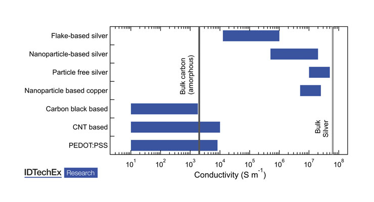
Conductive inks can be made from any material that is, well, conductive. Silver and carbon-based inks are the primary choices, with copper of interest. However, copper has issues with oxidation that make it less ideal for printing. Nanoparticle-based and particle-free alternatives are also emerging, but they are higher cost.
Dr. Matthew Dyson, technology analyst with IDTechEx, notes that IDTechEx estimates the current conductive ink market size as $2.3 billion, with silver the primary material for conductive inks.
“Almost 80% is silver flake-based ink that is used to make the conductive fingers on silicon solar panels,” Dr. Dyson reported. “While the market for this application is established and may even decline in the future as new technologies are adopted, there is extensive growth in flake-based inks for other applications, and also in emerging categories of conductive inks such as nanoparticle-based and particle-free inks.”
Khasha Ghaffarzadeh, CEO of TechBlick, a year-round event series with more than 350+ analyst selected live online presentations and 10-plus masterclasses, talked about the latest dynamics of the conductive inks market.
“Conductive inks are found in anything from a baby diaper to a precision missile,” Ghaffarzadeh said. “This makes the market wonderfully diverse and excellent at always adapting itself, rejuvenating itself, and re-inventing itself.”
Photovoltaics is the largest market, as conductive materials are used on the back of solar cells. Aside from photovoltaics, sensors, wearables and in-mold electronics are potentially sizable markets.
“This market is growing,” said Ghaffarzadeh. “Broadly speaking, we can talk of established and emerging applications. In the latter bucket, we have the huge, almost irreplaceable, solar cell market as well as other important markets like printed HMIs, LTCC metallization, and others.
“Those are fundamental to the industry, but the excitement is really in the emerging applications. Now here I could list many opportunities such as in-mold electronics, eTextiles, 5G filters, EMI shielding, sintered die attach paste, electrodes and skin patches, electrodes in CGMs and other biosensors, uLED substrate metallization, and many more,” Ghaffarzadeh added.
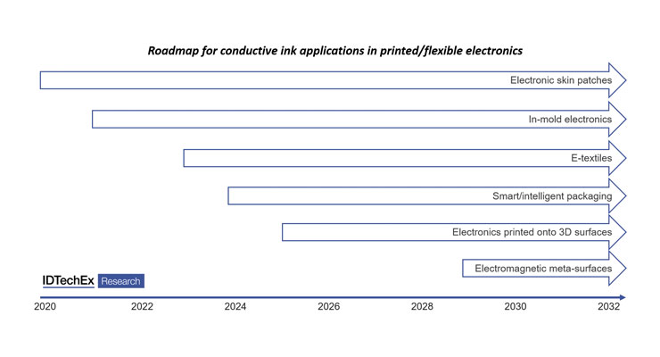
“In the near term, the biggest growth opportunities would appear to be wearable electronic skin patches and in-mold electronics,” Dr. Dyson observed. “Electronic skin patches require stretchable conductive ink, along with printed conductive electrodes in many cases, and are projected by IDTechEx to reach a market size of $38 billion by 2030.
“In-mold electronics (IME), and the closely related film-insert molding, is another application opportunity. Integrating electronics within plastic panels reduces weight, complexity and assembly costs. IME is thus highly applicable to automotive interiors, household appliances and even some consumer goods,” he added.
Toward the end of the decade, Dr. Dyson sees applications in partially additive electronics manufacturing, for example, printing wiring onto existing 3D structures, and also in smart packaging.
“Even further into the future, electromagnetic meta-surfaces that assist in the propagation and directing of the higher frequencies that will be used for telecommunications may represent a huge market for conductive ink,” he noted.
“The wide variety of applications for printed electronics means that there are many opportunities for differentiation within conductive inks,” Dr. Dyson noted. “Wearable electronics require inks that are stretchable to various extents and can withstand repeated mechanical flexing. The requirements for IME are slightly different, in that inks need to withstand the temperature and pressure associated with thermoforming.
However, there are still requirements that conductive ink manufacturers need to address. Dr. Florian Ullrich, business developer with InnovationLab, said that there are several important factors when selecting conductive inks. In particular, Dr. Ullrich pointed to price and availability, delivery time and shelf life, adhesion to substrate, scratch resistance and batch to batch reproducibility as important aspects when InnovationLab selects inks.
Dr. Ullrich noted that there are areas where conductive inks can be improved, beginning with less hazardous solvents, lower curing temperature or UV curing, higher material load and higher conductivity, and a long time for handling without drying.
“Considering conductive inks more broadly, the main challenges are durability and cost,” added Dr. Dyson. “Utilizing printed inks in harsh environments, such as automotive applications, means that they need to withstand repeated thermal cycling from -40°C to 80°C, while of course, silver-based inks are vulnerable to metal price rises.”
The Price of Silver Inks
That silver price volatility can be significant. Silver prices have been fluctuating wildly. On March 25, 2011, for example, silver prices were $25.165 per ounce according to Comex. The 52-week range was $13.90 to $30.16.
IDTechEx’s analysts say that rising silver metal prices could lead to changes in the composition of conductive ink markets.
“The most obvious is an acceleration in the transition from silver to copper, with the latter metal currently over 100x cheaper at around $8/kg,” IDTechEx’s analysts reported. “This price differential means that replacing silver with copper has long been highly desirable. However, it has proved extremely challenging since copper is far more reactive than silver and oxidizes relatively quickly in the air to insulating copper oxide (illustrated by green copper roofs and statues).”
Future of Printed And Flexible Electronics
Generally speaking, it seems like more products featuring printed and flexible electronics are reaching the marketplace.
“Printed electronics is growing, but not uniformly and not across all applications,” Ghaffarzadeh said. “This is no surprise given the tremendous diversity of the field. In fact, your measure of growth depends on how one defines the field of printed electronics.”
Dr. Dyson said he is seeing signs of growth in the field, and observed that there promising markets for flexible and printed electronics.
“There is substantial overlap between the most promising markets for printed/flexible electronics and conductive inks,” he added. “As such, electronic skin patches and in-mold electronics are especially promising applications in the near and medium-term, while smart packaging is a compelling long-term prospect.
“Flexible hybrid electronics (FHE) is another exciting opportunity for conductive ink, since it will enable printed inks to be utilized within circuits that combine mounted components with printed conductive traces, and thus can replace PCBs for applications where flexibility and lightweight are important,” Dr. Dyson noted. “IoT devices are also a highly promising market since they are likely to require both printed/flexible sensors and energy harvesting technologies such as indoor organic photovoltaics.”
Conductive inks can be made from any material that is, well, conductive. Silver and carbon-based inks are the primary choices, with copper of interest. However, copper has issues with oxidation that make it less ideal for printing. Nanoparticle-based and particle-free alternatives are also emerging, but they are higher cost.
Dr. Matthew Dyson, technology analyst with IDTechEx, notes that IDTechEx estimates the current conductive ink market size as $2.3 billion, with silver the primary material for conductive inks.
“Almost 80% is silver flake-based ink that is used to make the conductive fingers on silicon solar panels,” Dr. Dyson reported. “While the market for this application is established and may even decline in the future as new technologies are adopted, there is extensive growth in flake-based inks for other applications, and also in emerging categories of conductive inks such as nanoparticle-based and particle-free inks.”
Khasha Ghaffarzadeh, CEO of TechBlick, a year-round event series with more than 350+ analyst selected live online presentations and 10-plus masterclasses, talked about the latest dynamics of the conductive inks market.
“Conductive inks are found in anything from a baby diaper to a precision missile,” Ghaffarzadeh said. “This makes the market wonderfully diverse and excellent at always adapting itself, rejuvenating itself, and re-inventing itself.”
Photovoltaics is the largest market, as conductive materials are used on the back of solar cells. Aside from photovoltaics, sensors, wearables and in-mold electronics are potentially sizable markets.
“This market is growing,” said Ghaffarzadeh. “Broadly speaking, we can talk of established and emerging applications. In the latter bucket, we have the huge, almost irreplaceable, solar cell market as well as other important markets like printed HMIs, LTCC metallization, and others.
“Those are fundamental to the industry, but the excitement is really in the emerging applications. Now here I could list many opportunities such as in-mold electronics, eTextiles, 5G filters, EMI shielding, sintered die attach paste, electrodes and skin patches, electrodes in CGMs and other biosensors, uLED substrate metallization, and many more,” Ghaffarzadeh added.
“In the near term, the biggest growth opportunities would appear to be wearable electronic skin patches and in-mold electronics,” Dr. Dyson observed. “Electronic skin patches require stretchable conductive ink, along with printed conductive electrodes in many cases, and are projected by IDTechEx to reach a market size of $38 billion by 2030.
“In-mold electronics (IME), and the closely related film-insert molding, is another application opportunity. Integrating electronics within plastic panels reduces weight, complexity and assembly costs. IME is thus highly applicable to automotive interiors, household appliances and even some consumer goods,” he added.
Toward the end of the decade, Dr. Dyson sees applications in partially additive electronics manufacturing, for example, printing wiring onto existing 3D structures, and also in smart packaging.
“Even further into the future, electromagnetic meta-surfaces that assist in the propagation and directing of the higher frequencies that will be used for telecommunications may represent a huge market for conductive ink,” he noted.
“The wide variety of applications for printed electronics means that there are many opportunities for differentiation within conductive inks,” Dr. Dyson noted. “Wearable electronics require inks that are stretchable to various extents and can withstand repeated mechanical flexing. The requirements for IME are slightly different, in that inks need to withstand the temperature and pressure associated with thermoforming.
However, there are still requirements that conductive ink manufacturers need to address. Dr. Florian Ullrich, business developer with InnovationLab, said that there are several important factors when selecting conductive inks. In particular, Dr. Ullrich pointed to price and availability, delivery time and shelf life, adhesion to substrate, scratch resistance and batch to batch reproducibility as important aspects when InnovationLab selects inks.
Dr. Ullrich noted that there are areas where conductive inks can be improved, beginning with less hazardous solvents, lower curing temperature or UV curing, higher material load and higher conductivity, and a long time for handling without drying.
“Considering conductive inks more broadly, the main challenges are durability and cost,” added Dr. Dyson. “Utilizing printed inks in harsh environments, such as automotive applications, means that they need to withstand repeated thermal cycling from -40°C to 80°C, while of course, silver-based inks are vulnerable to metal price rises.”
The Price of Silver Inks
That silver price volatility can be significant. Silver prices have been fluctuating wildly. On March 25, 2011, for example, silver prices were $25.165 per ounce according to Comex. The 52-week range was $13.90 to $30.16.
IDTechEx’s analysts say that rising silver metal prices could lead to changes in the composition of conductive ink markets.
“The most obvious is an acceleration in the transition from silver to copper, with the latter metal currently over 100x cheaper at around $8/kg,” IDTechEx’s analysts reported. “This price differential means that replacing silver with copper has long been highly desirable. However, it has proved extremely challenging since copper is far more reactive than silver and oxidizes relatively quickly in the air to insulating copper oxide (illustrated by green copper roofs and statues).”
Future of Printed And Flexible Electronics
Generally speaking, it seems like more products featuring printed and flexible electronics are reaching the marketplace.
“Printed electronics is growing, but not uniformly and not across all applications,” Ghaffarzadeh said. “This is no surprise given the tremendous diversity of the field. In fact, your measure of growth depends on how one defines the field of printed electronics.”
Dr. Dyson said he is seeing signs of growth in the field, and observed that there promising markets for flexible and printed electronics.
“There is substantial overlap between the most promising markets for printed/flexible electronics and conductive inks,” he added. “As such, electronic skin patches and in-mold electronics are especially promising applications in the near and medium-term, while smart packaging is a compelling long-term prospect.
“Flexible hybrid electronics (FHE) is another exciting opportunity for conductive ink, since it will enable printed inks to be utilized within circuits that combine mounted components with printed conductive traces, and thus can replace PCBs for applications where flexibility and lightweight are important,” Dr. Dyson noted. “IoT devices are also a highly promising market since they are likely to require both printed/flexible sensors and energy harvesting technologies such as indoor organic photovoltaics.”
