03.29.12
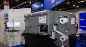
RadTech, the non-profit trade association for ultraviolet and electron beam (UV and EB) technologies, is again honoring innovative companies that utilize the fast emerging industrial process.
UV and EB technology offers fast throughput, superior product performance, energy efficiency and environmentally proactive processes that exemplify the enabling and paradigm shifting use of the technology in manufacturing and research and development.
The RadTech Emerging Technology Committee will recognize these companies at RadTech 2012, the biennial UV and EB Technology Conference and Exhibition, April 30 to May 2, in Chicago, www.radtech2012.com.
Some of these companies will also be presenting within the RadTech Conference to offer attendees the opportunity to learn how to move their business forward utilizing UV and EB Curing technology.
Award winners include:
• Conductive Film Manufactured using a Low Cost UV Curable Transparent, Roll to Roll Process by Micro and Nano-Embossing: UniPixel Inc., The Woodlands, TX.
Today's electronic devices can be thought of as a complex stack of layers or films. One of the most critical functions of a film in an electronic device is that of conductivity. The dominant technology used for transparent conductive films are thin films of ITO.
However, ITO has several major problems such as cost, future availability, brittleness and flexibility. UniPixel has taken a novel approach in solving these problems, offering a significant advantage over the production of most other conductive films. In addition to their conductive film solution, UniPixel has taken the concept of micro or nano-embossing UV curable films to develop anti-fingerprint and security films, and has also developed a high performance, hard, but flexible coating now being targeted as a protective layer for devices such as touch screens. UniPixel's innovate films are being tested in a large range of products, including touch screens, cell phones, 2D and 3D television and PVs. The key is that all of these unique products have been enabled by using UV curable materials and coatings.
• EB Coatings for Decorative Laminates on Film Substrates: Interprint NA, Pittsfield MA.
Interprint is a worldwide leading designer and printer of decorative papers used as the design layer in laminate surfaces such as kitchen countertops, flooring, furniture and retail fixtures. To supplement this paper-based business, the company recently invested in equipment that cures coatings that have been applied to a printed oriented polypropylene (OPP) with an electron beam. The resultant product provides excellent moisture and scratch/abrasion resistance. It also offers exceptional print fidelity, mitre foldability and gloss with low energy consumption, carbon footprint and cost.
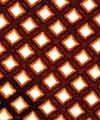
• UV Used to make the World's Lightest Structure: HRL Laboratories, LLC, Malibu, CA.
A new UV photopolymerization technique has been developed to create or "architect" microlattice materials in a rapid, scalable fashion. The microlattice materials are formed by taking advantage of a self-propagating waveguide phenomenon that can occur under certain exposure conditions. Because the waveguides propagate from a single exposure plane and can interconnect during formation, thick three-dimensional polymer microlattice materials can be formed in less than one minute with features ranging from tens of microns to millimeters.
The utility of these new materials range from lightweight energy absorbing structures to thermal management materials to bio-scaffolds. These materials have also been utilized to create the world's lightest structure enabled by UV technology.
To attend, or for information on the awards ceremony for these companies, as well as the technology Conference and Exposition, please visit www.radtech2012.com.
UV and EB technology offers fast throughput, superior product performance, energy efficiency and environmentally proactive processes that exemplify the enabling and paradigm shifting use of the technology in manufacturing and research and development.
The RadTech Emerging Technology Committee will recognize these companies at RadTech 2012, the biennial UV and EB Technology Conference and Exhibition, April 30 to May 2, in Chicago, www.radtech2012.com.
Some of these companies will also be presenting within the RadTech Conference to offer attendees the opportunity to learn how to move their business forward utilizing UV and EB Curing technology.
Award winners include:
• Conductive Film Manufactured using a Low Cost UV Curable Transparent, Roll to Roll Process by Micro and Nano-Embossing: UniPixel Inc., The Woodlands, TX.
Today's electronic devices can be thought of as a complex stack of layers or films. One of the most critical functions of a film in an electronic device is that of conductivity. The dominant technology used for transparent conductive films are thin films of ITO.
However, ITO has several major problems such as cost, future availability, brittleness and flexibility. UniPixel has taken a novel approach in solving these problems, offering a significant advantage over the production of most other conductive films. In addition to their conductive film solution, UniPixel has taken the concept of micro or nano-embossing UV curable films to develop anti-fingerprint and security films, and has also developed a high performance, hard, but flexible coating now being targeted as a protective layer for devices such as touch screens. UniPixel's innovate films are being tested in a large range of products, including touch screens, cell phones, 2D and 3D television and PVs. The key is that all of these unique products have been enabled by using UV curable materials and coatings.
• EB Coatings for Decorative Laminates on Film Substrates: Interprint NA, Pittsfield MA.
Interprint is a worldwide leading designer and printer of decorative papers used as the design layer in laminate surfaces such as kitchen countertops, flooring, furniture and retail fixtures. To supplement this paper-based business, the company recently invested in equipment that cures coatings that have been applied to a printed oriented polypropylene (OPP) with an electron beam. The resultant product provides excellent moisture and scratch/abrasion resistance. It also offers exceptional print fidelity, mitre foldability and gloss with low energy consumption, carbon footprint and cost.
• UV Used to make the World's Lightest Structure: HRL Laboratories, LLC, Malibu, CA.
A new UV photopolymerization technique has been developed to create or "architect" microlattice materials in a rapid, scalable fashion. The microlattice materials are formed by taking advantage of a self-propagating waveguide phenomenon that can occur under certain exposure conditions. Because the waveguides propagate from a single exposure plane and can interconnect during formation, thick three-dimensional polymer microlattice materials can be formed in less than one minute with features ranging from tens of microns to millimeters.
The utility of these new materials range from lightweight energy absorbing structures to thermal management materials to bio-scaffolds. These materials have also been utilized to create the world's lightest structure enabled by UV technology.
To attend, or for information on the awards ceremony for these companies, as well as the technology Conference and Exposition, please visit www.radtech2012.com.